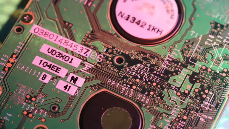
A printed circuit board (PCB) serves as the backbone of any electronic device. It is a bare board made of insulating material with conductive pathways etched onto its surface. On the other hand, a PCBA board is the next step in the process. It is a fully assembled and functional board where components like resistors, capacitors, and microchips are mounted onto the PCB.
The distinction between PCB and PCBA lies in their roles. A PCB provides the structure and wiring for circuits, while a PCBA brings the board to life by adding functionality. Understanding this difference is essential for engineers and manufacturers. Each phase of production comes with unique challenges, from designing the PCB to assembling and testing the PCBA.
The global PCB market reflects the growing demand for these technologies. Analysts valued it at over $78 billion in 2021 and expect it to reach $128 billion by 2030. This growth highlights the importance of recognizing the roles of PCB and PCBA in modern electronics manufacturing.
Key Takeaways
- A PCB is an empty board with paths for electricity. A PCBA is a board with parts that do specific jobs.
- Knowing the difference between PCB and PCBA helps engineers and makers pick the right one for their work.
- PCBs are great for trying out ideas and testing. PCBAs are used in working devices like phones and medical tools.
- Picking the right way to put parts on, like Surface Mount or Through-Hole, changes how well it works and its cost.
- Testing and checking during PCB and PCBA steps find problems early. This makes sure devices work well and last long.
What is a PCB?
Definition of PCB
A printed circuit board (PCB) is a foundational component in electronics. It connects electronic components using copper conductors and provides mechanical support for mounting them. PCBs consist of alternating layers of conductive copper and insulating material. These layers are laminated together to form a rigid structure. The conductive features include copper traces, pads, and planes, which enable electrical connections. A solder mask covers the surface to prevent short circuits, while a silk screen identifies components.
PCBs are essential for creating compact and efficient electronic devices. Without them, modern electronics would be bulky and unreliable.
Components of a PCB
Every PCB includes several key materials that determine its performance:
- Prepreg: A tacky material that bonds laminates or foils.
- Copper foil: Acts as the conductor for electrical signals.
- Copper-clad laminates: Combine prepregs and copper foils, forming the PCB’s core.
These materials influence the PCB’s thermal, electrical, and mechanical properties. For example, thermal conductivity ensures heat dissipation, while mechanical strength enhances durability.
| Material | Function |
|---|---|
| Prepreg | Bonds laminates or foils. |
| Copper foil | Conducts electrical signals. |
| Copper Clad Laminates | Forms the PCB’s structural core. |
Types of PCBs
PCBs come in various types, each suited for specific applications.
Single-layer PCB
A single-layer PCB has one conductive layer. It is simple and cost-effective, making it ideal for basic devices like calculators and LED lights.
Multi-layer PCB
Multi-layer PCBs consist of multiple conductive layers separated by insulating materials. These are essential for complex electronics requiring high circuit density. They offer enhanced functionality, durability, and compactness. Devices like smartphones and computers rely on multi-layer PCBs for their advanced features.
Flexible PCB
Flexible PCBs use bendable materials, allowing them to fit into compact or irregular spaces. They are common in wearable devices and medical equipment. Their flexibility reduces the risk of damage during operation.
Each type of PCB plays a unique role in electronics, ensuring optimal performance for different devices.
PCB Manufacturing Process
Design and layout
The PCB manufacturing process begins with design and layout. You start by creating a schematic diagram that outlines the circuit’s functionality. Specialized software like Eagle or Altium Designer helps you translate this schematic into a physical layout. This layout determines the placement of components and the routing of copper traces.
The substrate material forms the base of the PCB. It provides a sturdy and dust-resistant foundation. A copper-sided laminate is cleaned thoroughly to remove contaminants. This ensures a clean surface for the next steps. A layer of photo-sensitive film, known as photo resist, is applied. When exposed to UV light, the photo resist hardens, matching the design precisely.
Etching and layering
Etching removes unwanted copper from the board. After applying the photo resist, the board is washed with an alkaline solution to eliminate any unhardened areas. A pressure wash follows to ensure no residue remains. The hardened photo resist protects the desired copper during this process.
Next, the layers of the PCB are aligned. Registration holes and an optical punch ensure precise alignment. The layers are then fused together through a bonding process. This step creates a multi-layer PCB if required. Holes are drilled into the stack with high precision to prepare for component placement.
Quality testing
Quality testing ensures the PCB meets design specifications. Automatic optical inspection compares the board to the original design. This step identifies defects like missing traces or misaligned layers. Electrical tests confirm the functionality of the PCB. These tests verify that the copper traces conduct electricity as intended.
Common challenges during manufacturing include soldering defects, acid traps, and slivers. You can address these issues by implementing rigorous quality control measures and using advanced manufacturing techniques. For example, automated inspection systems help detect missing solder masks, while laser cutting minimizes slivers.
A well-tested PCB ensures reliability and performance in the final product.
What is a PCBA?
Definition of PCBA
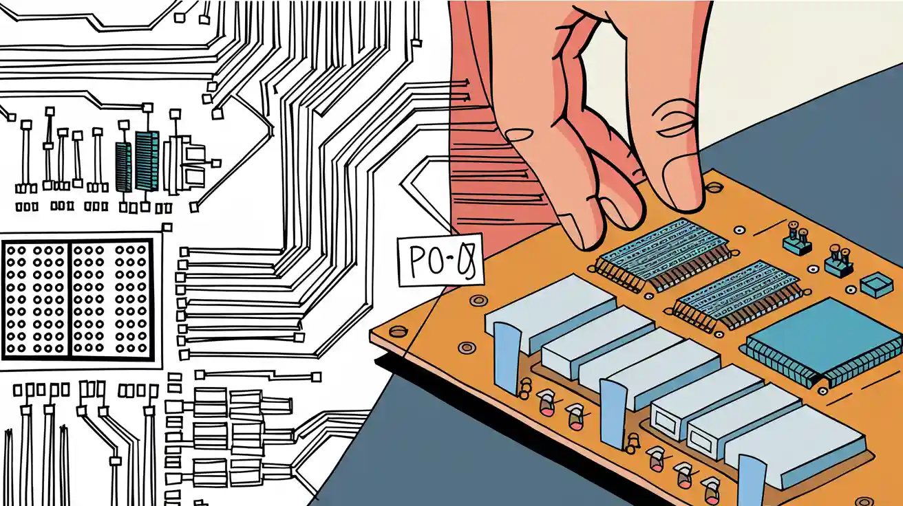
A PCBA, or Printed Circuit Board Assembly, is the stage where a bare PCB transforms into a functional circuit. This process involves mounting and soldering electronic components like resistors, capacitors, and integrated circuits onto the PCB. While a PCB provides the structural foundation, the PCBA board performs the intended electronic functions.
| Aspect | PCB (Printed Circuit Board) | PCBA (Printed Circuit Board Assembly) |
|---|---|---|
| Definition | Bare, unpopulated board providing electrical connections | Populated PCB with electronic components, forming a functional circuit |
| Function | Mechanical support and electrical pathways for components | Performs a specific electronic function |
| Components | None (empty board) | All necessary electronic components (resistors, capacitors, ICs, etc.) |
Components of a PCBA
A PCBA board includes several critical components that enable its functionality:
| Component | Function |
|---|---|
| Resistors | Limit the flow of electrical current, ensuring safe operation of other components. |
| Capacitors | Store and release electrical energy, crucial for filtering and stabilizing power supply. |
| Integrated Circuits | Compact devices containing numerous electronic components to perform complex functions. |
| Connectors | Provide interfaces for communication and power transfer between the PCBA and other systems. |
Each component plays a vital role in ensuring the PCBA operates efficiently and reliably. For example, resistors protect sensitive parts by controlling current flow, while capacitors stabilize voltage levels.
Printed Circuit Board Assembly Methods
The assembly of a PCBA involves different techniques, each suited for specific applications.
Surface Mount Technology (SMT)
SMT is the most common method for assembling a PCBA board. Components are mounted directly onto the surface of the PCB without requiring holes. This technique allows for higher component density and supports two-sided assembly. Automated machines handle the placement, making SMT efficient and precise.
Through-Hole Technology (THT)
THT involves inserting component leads through pre-drilled holes in the PCB. This method provides strong mechanical bonds, making it ideal for applications requiring durability, such as industrial equipment. However, it typically results in a larger PCB footprint and is less suited for compact designs.
| Through-Hole | Surface Mount |
|---|---|
| Requires holes for component leads | Components mount directly to surface pads |
| Typically larger footprint | Minimal PCB footprint |
| Manual assembly common | Automated assembly preferred |
| Lower component density | Higher component density |
| 2-sided assembly rare | 2-sided assembly common |
Mixed Technology
Mixed technology combines SMT and THT to leverage the advantages of both methods. For instance, you might use SMT for compact components and THT for parts requiring mechanical strength. This approach ensures flexibility and adaptability in PCB assembly.
Modern advancements in PCBA assembly, such as automation and robotics, have further improved efficiency. Automated systems enhance precision, reduce errors, and increase throughput, making them indispensable in high-volume production.
By understanding these methods, you can choose the right approach for your PCBA board, ensuring optimal performance and cost-effectiveness.
PCBA Testing and Quality Assurance
Functional Testing
Functional testing ensures that the PCBA operates as intended under real-world conditions. This process evaluates the board’s performance by simulating its actual working environment. You can use this method to verify that all components interact correctly and meet design specifications. For example, functional testing might involve powering the PCBA and running specific software to check its response.
One of the most common techniques for functional testing is In-Circuit Testing (ICT). ICT uses electrical probes to detect issues like short circuits, open circuits, or incorrect component placement. Another effective method is Flying Probe Testing (FPT). This approach employs movable probes to test electrical continuity and component functionality without requiring a custom fixture.
Functional testing is critical for identifying defects that could affect the PCBA’s performance. By addressing these issues early, you can ensure the reliability and efficiency of your final product.
Visual Inspection
Visual inspection is one of the simplest yet most effective methods for ensuring the quality of a PCB assembly. This process involves examining the PCBA for visible defects, such as soldering errors, misaligned components, or damaged traces. You can perform this inspection manually or use automated systems for greater accuracy.
Automated Optical Inspection (AOI) is a popular choice for visual inspection. It uses high-resolution cameras to capture detailed images of the PCBA. The system then compares these images to the original design to identify any discrepancies. X-ray inspection is another advanced technique. It allows you to detect hidden defects, such as voids in solder joints or issues in multilayer PCBs.
By combining manual and automated methods, you can achieve a thorough inspection of your PCBA. This step is essential for maintaining high-quality standards and preventing costly errors in production.
Tip: Regular visual inspections during the PCB assembly process can help you catch defects early, saving time and resources.
PCB vs PCBA: Key Differences
Comparison Table
Understanding the differences between a PCB and a PCBA becomes easier when you compare their key attributes side by side.
| Aspect | PCB (Printed Circuit Board) | PCBA (Printed Circuit Board Assembly) |
|---|---|---|
| Composition | Fiberglass substrate with copper traces | PCB with mounted electronic components and solder connections |
| Functionality | Provides mechanical structure and electrical pathways | Performs specific electronic functions |
| Testing | Tested for continuity and shorts | Undergoes comprehensive testing for functionality |
This table highlights how a PCB serves as the foundation, while a PCBA represents the complete, functional assembly.
Differences in Functionality
A PCB acts as the skeleton of an electronic device. It provides the mechanical support and electrical pathways needed to connect components. However, it cannot perform any electronic function on its own.
In contrast, a PCBA transforms the bare PCB into a working circuit. By mounting components like resistors, capacitors, and integrated circuits, the PCBA becomes capable of performing specific tasks. For example, a PCBA in a smartphone enables features like touch sensitivity and wireless communication.
Think of a PCB as a blank canvas and a PCBA as the finished painting. The PCB lays the groundwork, but the PCBA brings the design to life.
Differences in Manufacturing Processes
The manufacturing processes for PCBs and PCBAs differ in complexity and cost. Producing a PCB involves simpler steps like designing, etching, and layering. These steps result in a bare board that costs less and takes less time to manufacture.
Creating a PCBA adds several layers of complexity. You need to procure components, assemble them onto the PCB, and perform rigorous testing. These additional steps increase production costs and lead times. For instance, while a bare PCB might cost $5, the total cost of a PCBA, including components and labor, could reach $30.
The assembly process also requires precision. Techniques like Surface Mount Technology (SMT) and Through-Hole Technology (THT) ensure components are securely attached. Testing methods like functional testing and visual inspection further guarantee the PCBA’s reliability.
Choosing between a PCB and a PCBA depends on your project’s requirements. If you need a functional circuit, a PCBA is the way to go. However, for prototyping or basic designs, a PCB might suffice.
Differences in Applications
The applications of PCBs and PCBAs vary significantly due to their distinct roles in electronics. A PCB serves as the foundation for electronic circuits. It provides the structure and pathways for electrical connections. You will often find PCBs used in prototyping and testing phases. Engineers rely on them to design and evaluate circuits before moving to full production. For example, a single-layer PCB might be used to test a simple LED circuit.
On the other hand, a PCBA is the complete, functional assembly. It powers the devices you use daily. PCBAs are essential in consumer electronics like smartphones, laptops, and gaming consoles. They also play a critical role in industrial equipment, medical devices, and automotive systems. For instance, the PCBA in a car’s engine control unit ensures optimal performance by managing fuel injection and ignition timing.
The complexity of the application often determines whether you need a PCB or a PCBA. If you are working on a basic project or prototype, a PCB might suffice. However, for a finished product that requires functionality, you will need a PCBA. This distinction is crucial when planning your project. It helps you allocate resources effectively and meet your design goals.
Tip: Always consider the end-use of your project when deciding between a PCB and a PCBA. This choice can impact cost, production time, and overall performance.
Applications and Use Cases
When to Use a PCB
You should use a PCB when you need a foundational platform for designing and testing electronic circuits. PCBs are ideal during the prototyping phase, where engineers focus on creating and refining circuit layouts. They are also preferred in applications where assembly is unnecessary, such as testing equipment for firearms or marine navigation systems. In these cases, the PCB provides the structure and electrical pathways needed for evaluation without requiring additional components.
PCBs are also common in security systems like alarms and locks. Their simplicity and cost-effectiveness make them suitable for basic designs. For example, a single-layer PCB might be used in a basic alarm circuit to connect sensors and triggers.
When to Use a PCBA
You should opt for a PCBA when you need a fully functional electronic assembly. PCBAs are essential for devices that require integrated components to perform specific tasks. For instance, a PCBA in a smartphone enables features like touch sensitivity and wireless communication.
PCBAs are also critical in industries where reliability and performance are non-negotiable. Medical devices like pacemakers and CT scanners rely on PCBAs to function accurately and consistently. Similarly, automotive systems, such as engine control units and anti-lock brakes, depend on robust PCBAs to withstand harsh conditions and ensure safety.
Examples of Industries and Products
Consumer Electronics
Consumer electronics heavily rely on PCBAs for their compact and efficient designs. Smartphones, laptops, and gaming consoles all contain high-density multi-layer PCBAs. Home appliances like refrigerators and microwaves also use PCBAs to manage their electronic functions. Even entertainment systems, such as TVs and stereo sets, depend on PCBAs for seamless operation.
Automotive
Modern vehicles incorporate PCBAs in various systems to enhance performance and safety. Engine control units, infotainment systems, and advanced driver-assistance systems all utilize PCBAs. These assemblies must endure extreme temperatures and vibrations, making durability a key factor in their design.
Medical Devices
Medical devices demand the highest standards of reliability and precision. PCBAs are integral to devices like pacemakers, blood glucose monitors, and MRI machines. For example, a pacemaker contains a tiny PCBA that must operate flawlessly for years inside the human body. Scanning technologies, such as CT scanners and ultrasonic devices, also depend on PCBAs to deliver accurate results.
Tip: When choosing between a PCB and a PCBA, always consider the complexity and functionality required by your project. This decision will impact the cost, production time, and overall performance of your device.
Understanding the differences between PCB and PCBA is essential for making informed decisions in electronics design. A PCB serves as the structural base, while a PCBA is the fully assembled, functional circuit. Each plays a unique role in the product development lifecycle.
When deciding between the two, consider:
- The stage of your project.
- The desired functionality and complexity.
- Production scale and cost-effectiveness.
Choosing the right option ensures your project aligns with its goals. For simpler designs or prototyping, a PCB may suffice. For a complete, ready-to-use solution, a PCBA is the way to go.
Ultimately, a PCB is the starting point, but a PCBA transforms it into a functional masterpiece.
FAQ
What is the difference between a PCB and a PCBA?
A PCB is a bare board that provides the structure and electrical pathways for circuits. A PCBA, or circuit card assembly, includes the PCB with all necessary components mounted, making it a functional electronic assembly.
Why is PCB testing important?
Testing ensures the PCB meets design specifications and functions correctly. It identifies defects like short circuits or misaligned layers, which could affect the reliability of the final product.
How does Surface Mount Technology (SMT) differ from Through-Hole Technology (THT)?
SMT mounts components directly onto the PCB surface, allowing higher density and compact designs. THT involves inserting component leads through holes, providing stronger mechanical bonds but requiring more space.
What role does a PCBA play in the electronic manufacturing process?
A PCBA transforms a bare PCB into a functional circuit by adding components. It is a critical step in the electronic manufacturing process, ensuring the final product performs its intended functions.
Can a PCB be used without assembly?
Yes, a PCB can be used for prototyping or testing circuits. However, for a functional device, you need a PCBA with all components assembled and tested.