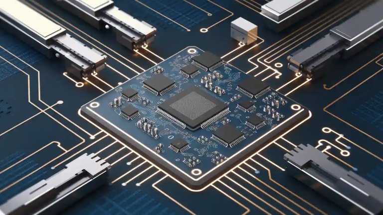
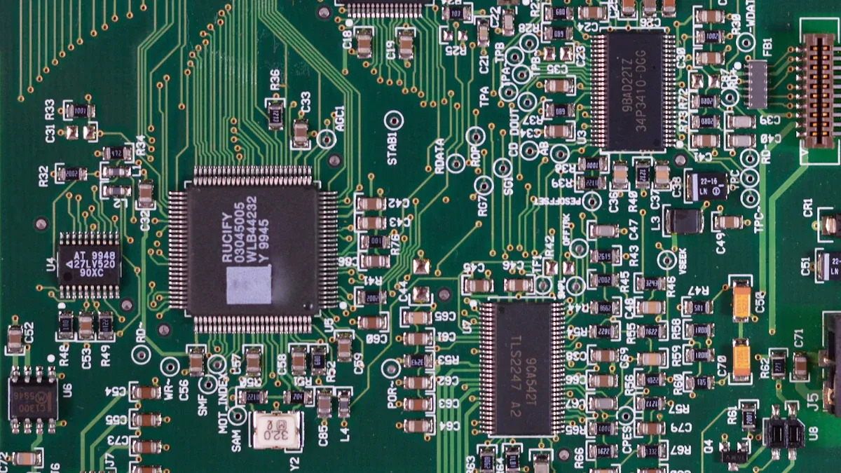
When you think about the compact and powerful devices you use daily, multilayer PCBs are the hidden heroes making them possible. Engineers craft these PCBs by stacking conductive and insulating materials under intense heat and pressure. This process creates a compact structure capable of handling complex electrical tasks.
The efficiency of multilayer PCB manufacturing has soared in recent years. Here’s why:
- The growing demand for high-performance, space-saving devices has driven advancements in PCB production.
- Manufacturers now use cutting-edge materials and techniques to boost both reliability and performance.
- Collaborations between industry leaders have accelerated innovation, paving the way for next-gen PCBs.
With this precision engineering, you get devices that are smaller, faster, and more reliable. Multilayer PCBs are the backbone of modern technology, ensuring your gadgets perform flawlessly.
Key Takeaways
- Multilayer PCBs are important for today’s electronics. They allow smaller designs and better features.
- Engineers pick the right materials and methods to make them work well.
- These PCBs lower signal problems, helping high-speed devices work better.
- Using multilayer PCBs makes building and testing easier. This saves time and money.
- The need for faster devices pushes new ideas in making multilayer PCBs.
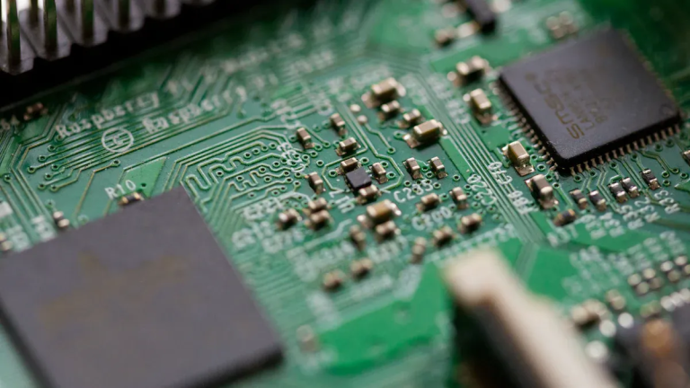
What Are Multilayer PCBs?
Multilayer PCBs are the foundation of modern electronics, enabling compact designs and advanced functionality. These printed circuit boards consist of multiple conductive layers separated by insulating materials, all bonded together in a precise stack-up. Their intricate design allows for efficient signal routing, reduced interference, and enhanced performance.
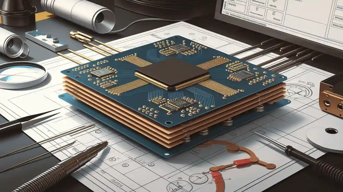
Structure and Layers
The structure of a multilayer PCB is a marvel of engineering. It typically includes alternating layers of conductive copper and insulating materials like epoxy resin or fiberglass. These layers are stacked and bonded under high pressure and temperature to form a unified board.
Here’s a breakdown of common configurations:
| Layer Count | Description | Benefits |
|---|---|---|
| 4-layer | Top, two inner (power and ground), and bottom layers. | Versatile for various designs, improves electromagnetic compatibility. |
| 6-layer | Adds two extra signal layers between the planes. | Helps manage EMI, separates high-speed and low-speed signals. |
| 8-layer | Features four signal layers and four planes (ground and power). | Minimizes crosstalk, enhances routing quality, suitable for complex devices. |
Each configuration serves specific purposes. For example, a 4-layer PCB is ideal for basic designs, while an 8-layer PCB excels in high-speed applications by reducing crosstalk and improving signal integrity.
Purpose in Electronics
Multilayer PCBs are indispensable in today’s technology-driven world. They support intricate electrical circuits and higher component density, making them essential for devices like smartphones, laptops, and medical equipment.
Their advanced design offers several benefits:
- Better Signal Integrity: Dedicated ground and power planes enhance signal quality.
- Reduced EMI: Multilayer designs minimize electromagnetic interference, ensuring reliable performance.
- Efficient Power Distribution: They handle complex power requirements with ease.
The rise of 5G networks and automated systems has further increased the demand for multilayer PCBs. These boards play a critical role in telecommunications, where efficient power distribution and minimal signal loss are paramount. By choosing multilayer PCBs, you ensure your devices meet the highest standards of performance and reliability.
Why Use Multilayer PCBs?
Key Advantages
Multilayer PCBs offer a range of benefits that make them the go-to choice for modern electronics. Their advanced design provides unmatched reliability and performance compared to traditional printed circuit boards. Here’s why you should consider them:
- Higher reliability due to the strong bonding between layers.
- Simplified assembly and testing processes, saving time and effort.
- Reduced costs by replacing multiple single-layer boards with one compact solution.
- Increased design flexibility, allowing last-minute modifications without hassle.
- Smaller size by utilizing vertical space in the stack-up, making devices more compact.
- Lighter construction while maintaining the ability to handle complex electrical circuits.
- Higher quality and density of connections, ensuring better performance.
- Improved durability, making them suitable for demanding applications.
- Simplified connections with a single termination point, reducing wiring complexity.
These advantages make multilayer PCBs indispensable for creating high-performance devices that meet the demands of today’s fast-paced world.
Applications in Modern Devices
Multilayer PCBs are at the heart of many cutting-edge technologies. Their ability to handle complex electrical requirements in a compact form makes them essential for various industries.
The market for multilayer PCBs is booming. In 2023, it reached $1.5 billion, and it’s projected to grow to $3.2 billion by 2032, with a CAGR of 8.7%. This growth is driven by the rising demand for miniaturization and high-density interconnect (HDI) technology.
You’ll find multilayer PCBs in a wide range of devices:
- Computers and Servers: Used in motherboards and graphics cards to support high-density designs.
- Telecommunications: Essential for networking equipment to manage high-speed data transmission.
- Medical Devices: Critical for advanced equipment like MRI machines and portable diagnostic tools.
- Aerospace and Defense: Necessary for avionics and radar systems to meet stringent performance standards.
The multilayer flexible PCB segment is also gaining traction. Advancements in manufacturing now allow for higher layer counts and enhanced functionality, making these PCBs vital for next-generation electronics. Industries like consumer electronics, automotive, and healthcare are driving this trend, as they require compact designs with complex electrical capabilities.
By choosing multilayer PCBs, you ensure your devices stay ahead of the curve, delivering the performance and reliability that modern users demand.
PCB Manufacturing Process: Step-by-Step
Material Selection
The foundation of any successful multilayer PCB lies in choosing the right materials. This step ensures your printed circuit boards meet the performance and durability requirements of their intended applications. Engineers carefully evaluate materials based on several critical criteria:
- High-Frequency Applications: Materials with a low dielectric constant and minimal signal loss are essential for maintaining signal integrity.
- Automotive and Aerospace Applications: These industries demand materials that can endure extreme temperatures and vibrations without compromising performance.
| Performance Criteria | Description |
|---|---|
| Thermal Performance | Measures heat dissipation efficiency through thermal conductivity and glass transition temperature (Tg). |
| Mechanical Strength | Assesses durability with tensile strength, impact resistance, and flexural strength. |
| Cost Considerations | Balances material performance with manufacturing and maintenance costs. |
| Environmental Considerations | Focuses on sustainable practices and minimizing material toxicity. |
When selecting materials, you should also consider specific properties like thermal conductivity, dielectric constant, and loss tangent. These factors directly impact the electrical performance and reliability of your multilayer PCB.
Inner Layer Imaging
Inner layer imaging is where the intricate electrical pathways of your PCB come to life. This step involves transferring the circuit design onto the inner layers of the board using advanced imaging techniques. Modern PCB fabrication processes rely on cutting-edge technologies to achieve high precision and resolution.
- Direct Imaging (DI) and Laser Direct Imaging (LDI) systems have revolutionized this stage. They offer superior feature resolution and registration accuracy compared to traditional methods.
- Advanced copper foils, such as ultra-thin and ultra-smooth variants, enhance the adhesion and uniformity of photoresist coatings. This improvement ensures consistent imaging quality and reliability.
- Statistical process control (SPC) techniques and design of experiments (DOE) help eliminate variations, resulting in higher yields and consistent quality.
These advancements allow you to create printed circuit boards with intricate designs and exceptional electrical performance, meeting the demands of modern electronics.
Etching and Cleaning
Etching and cleaning are crucial steps in the PCB manufacturing process. After imaging, the unwanted copper is removed from the inner layers to reveal the desired circuit patterns. This process requires precision to ensure the electrical pathways remain intact.
- Chemical Etching: A chemical solution removes excess copper, leaving behind the circuit traces. The etching process must be carefully controlled to prevent over-etching or under-etching, which can compromise the board’s functionality.
- Cleaning: After etching, the layers undergo thorough cleaning to remove any residues or contaminants. This step ensures the surface is pristine and ready for the next stage of the stack-up process.
By maintaining strict control during etching and cleaning, you can produce multilayer PCBs with accurate circuit patterns and reliable electrical performance.
Layer Lamination
Layer lamination is the heart of the multilayer PCB manufacturing process. This step bonds the individual layers into a single, unified structure, ensuring durability and electrical reliability. You achieve this by stacking the layers in a precise order and applying heat and pressure to fuse them together.
To validate the reliability of the lamination process, engineers use advanced performance metrics:
- Scanning Acoustic Microscopy (SAM): Detects voids or layer separation.
- Interconnect Stress Testing (IST): Evaluates the strength of interconnections under stress.
- Solder Float Testing: Assesses the impact of lamination during soldering.
- Reflow Simulation Testing: Simulates soldering stresses to ensure reliability.
Mechanical properties like thickness and delamination resistance are also critical. Internal stress relief techniques prevent deformations, while thermal reliability ensures the layers remain intact under high temperatures. These measures guarantee that your multilayer PCB performs flawlessly in demanding applications.
Drilling and Plating
Drilling and plating are pivotal in creating the electrical pathways that connect the layers of your PCB. Drilling begins with pinpoint accuracy, guided by X-ray machines to ensure the holes align perfectly with the circuit design. This precision maintains the integrity of the PCB stack and prevents misalignment.
Once drilled, the holes undergo electroplating. During this process, the PCB is submerged in an electrolytic bath, where copper is deposited onto the walls of the holes. This step creates robust interconnections between the layers, enhancing both functionality and structural integrity. The intricate nature of this fabrication process ensures your PCB can handle complex electrical circuits with ease.
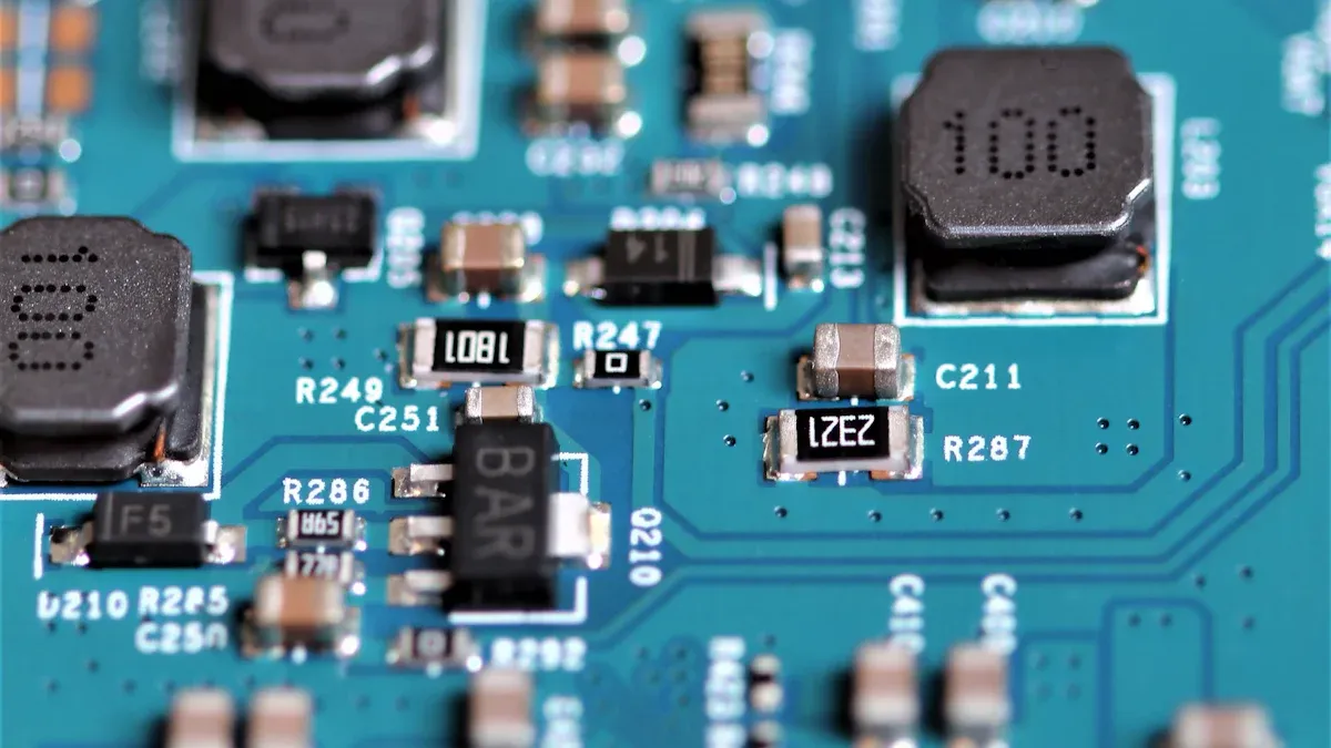
Surface Finishing and Solder Mask
Surface finishing and solder mask application are the final touches in the PCB fabrication process. These steps protect the board and prepare it for assembly. Surface finishes, such as HASL (Hot Air Solder Leveling) or ENIG (Electroless Nickel Immersion Gold), provide a smooth, solderable surface while preventing oxidation.
The solder mask, a protective layer, shields the PCB from environmental damage and prevents solder bridges during assembly. Quality control standards like IPC-6012 and IPC-SM-840 ensure proper adhesion and coverage. Adhesion testing confirms the solder mask sticks securely to the substrate, while coverage testing guarantees complete protection across the board. These measures ensure your PCB remains reliable and durable in real-world applications.
Final Assembly and Testing
The final assembly and testing stage is where your multilayer PCB comes to life. This step ensures that the board is fully functional and ready for integration into your devices. Engineers meticulously assemble components onto the PCB, following precise layouts to maintain accuracy and reliability.
Functional testing is the cornerstone of this stage. It validates that the assembled PCB operates as intended. Engineers perform solderability tests to confirm that all components are securely bonded. These tests include visual inspections and thermal cycling to ensure the solder joints can withstand real-world conditions.
Electrical testing is equally critical. Continuity tests verify that electrical connections are intact, while in-circuit testing identifies any faults in the assembly. These tests ensure that your PCB meets the highest standards of performance and reliability.
The process also includes quality checks to confirm that the PCB meets design specifications. Engineers use advanced tools to inspect the board for defects, such as misaligned components or damaged traces. Any issues are addressed promptly to maintain the integrity of the final product.
By the end of this stage, your PCB is not just a collection of layers and components. It becomes a fully functional unit, ready to power the devices that drive modern technology. This meticulous process ensures that your PCB delivers the performance and durability you expect.
Precision and Quality in Multi-Layer PCBs
Importance of Accuracy
Accuracy is the cornerstone of the pcb manufacturing process. When you aim for precision, you ensure that every layer aligns perfectly, creating a reliable and efficient circuit. Even the smallest misalignment can lead to signal loss, overheating, or complete failure of the device. This is why engineers prioritize accuracy at every stage of the process.
To highlight the importance of precision, consider these benchmarks:
| Metric | Value |
|---|---|
| PCB Yield Rate | 96% |
| Target Manufacturing Cycle Time | Reduction of 20% |
| Improvement in Overall Efficiency | Up to 15% |
These metrics demonstrate how accuracy directly impacts the reliability and efficiency of multilayer PCBs. By maintaining high yield rates and reducing cycle times, you not only save costs but also deliver products that meet the highest standards. Precision ensures that your devices perform flawlessly, even in demanding applications.
Quality Control Techniques
Quality control is essential for maintaining the reliability of multilayer PCBs. Advanced techniques ensure that every board meets strict performance criteria. One of the most effective methods involves integrating AI and convolutional neural networks (CNNs) into the inspection process. These technologies analyze high-resolution images to detect defects like soldering errors and misalignments. By automating defect detection, you achieve higher accuracy and faster inspection times.
In addition to AI-driven methods, engineers use rigorous testing protocols to validate the quality of PCBs. These include:
- Electrical Testing: Verifies the continuity and insulation of circuits.
- Thermal Stress Testing: Ensures the board can withstand extreme temperatures.
- X-Ray Inspection: Detects hidden defects within the layers.
These techniques not only improve defect detection rates but also enhance the overall reliability of the manufacturing process. By investing in quality control, you guarantee that your PCBs deliver consistent performance, even in critical applications.
| Metric | Multilayer PCBs | Double-Layer PCBs | Single-Layer PCBs |
|---|---|---|---|
| Signal Integrity | High | Moderate | Low |
| Thermal Management | Excellent | Good | Poor |
| Mechanical Strength | High | Moderate | Low |
| Environmental Impact | Material Waste | Energy Consumption | |
| 10-15% | 20-25% | 30-35% | |
| 15-20 kWh/kg | 10-15 kWh/kg | 5-10 kWh/kg |
By adopting these advanced quality control techniques, you ensure that your pcb manufacturing process produces boards with unmatched reliability and performance. This commitment to quality sets your products apart in a competitive market.
Multilayer PCBs are the backbone of modern electronics. They allow you to enjoy compact, high-performance devices that power your daily life. From smartphones to medical equipment, these PCBs ensure reliability and efficiency in every application.
The manufacturing process demands precision at every step. Engineers use advanced techniques to create PCBs that meet the highest standards of quality. Their expertise ensures your devices perform flawlessly, even in the most demanding environments.
By choosing multilayer PCBs, you invest in technology that delivers unmatched performance and durability. Trust in the expertise of engineers to bring your innovations to life.
FAQ
What makes multilayer PCBs better than single-layer ones?
Multilayer PCBs offer higher reliability, better signal integrity, and compact designs. They handle complex circuits efficiently, making them ideal for modern devices. By choosing multilayer PCBs, you ensure your products meet the demands of advanced technology and deliver superior performance.
How do engineers ensure the quality of multilayer PCBs?
Engineers use advanced quality control techniques like X-ray inspection, thermal stress testing, and AI-driven defect detection. These methods guarantee that every PCB meets strict performance standards. You can trust these processes to deliver reliable and durable boards for your devices.
Are multilayer PCBs suitable for high-temperature environments?
Yes, multilayer PCBs are designed to withstand extreme conditions. Engineers select materials with high thermal conductivity and durability. This ensures your PCBs perform reliably in demanding applications like aerospace, automotive, and industrial equipment.
Can multilayer PCBs reduce electromagnetic interference (EMI)?
Absolutely! Multilayer PCBs minimize EMI by incorporating dedicated ground and power planes. This design improves signal integrity and ensures stable performance. By using these PCBs, you can achieve better functionality in high-speed and sensitive electronic devices.
Why should you invest in multilayer PCBs for your projects?
Multilayer PCBs save space, improve performance, and simplify assembly. They support complex designs while reducing costs in the long run. By investing in these PCBs, you future-proof your devices and stay ahead in a competitive market.