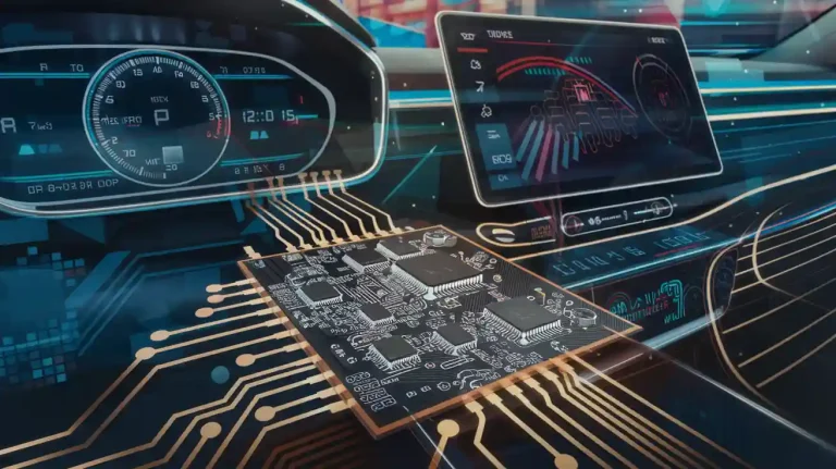
The assembly PCB SMT process revolutionises how printed circuit boards (PCBs) are manufactured. It involves mounting electronic components directly onto the surface of a PCB, eliminating the need for traditional through-hole methods. This innovation has become indispensable in modern electronics manufacturing due to its ability to enhance production efficiency and minimise errors.
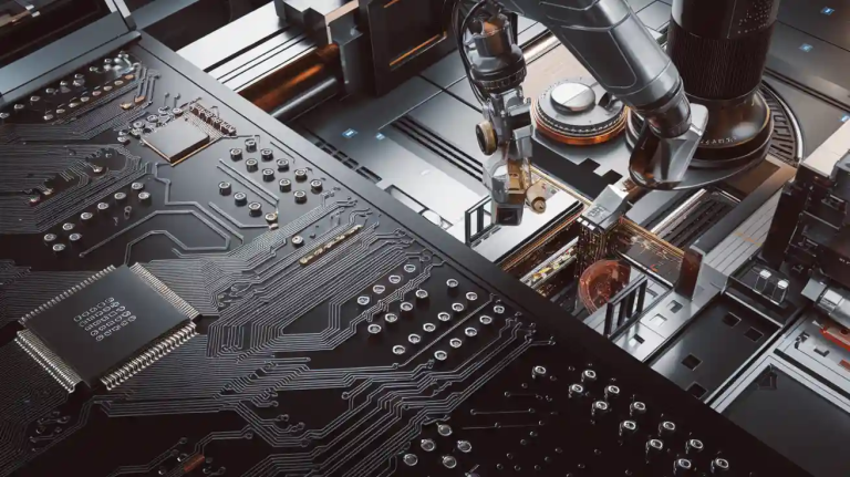
Automation plays a pivotal role in making assembly PCB SMT highly effective. Advanced machinery ensures faster assembly, higher precision, and reduced defects, resulting in compact, efficient, and reliable PCBs. For instance, SMT components are smaller and lighter, enabling designs with higher component density. This is crucial for devices like smartphones, wearables, and other space-constrained electronics.
📊 The global assembly PCB SMT equipment industry was valued at US$ 5.7 billion in 2022 and is projected to grow to US$ 9.1 billion by 2031, driven by increasing demand for consumer electronics. Asia Pacific dominates the market, holding 42.8% of the share.
This cutting-edge technology continues to shape the future of electronics, offering manufacturers a pathway to innovate and excel in a competitive landscape.
Key Takeaways
- Surface Mount Technology (SMT) helps make PCBs smaller and better by placing parts directly on the surface.
- Using machines in SMT assembly makes production faster, cheaper, and more reliable by reducing mistakes.
- Double-sided SMT assembly allows more parts and complex designs. It is great for modern gadgets but needs good planning and checks.
Overview of Surface Mount Technology
What Is Surface Mount Technology?
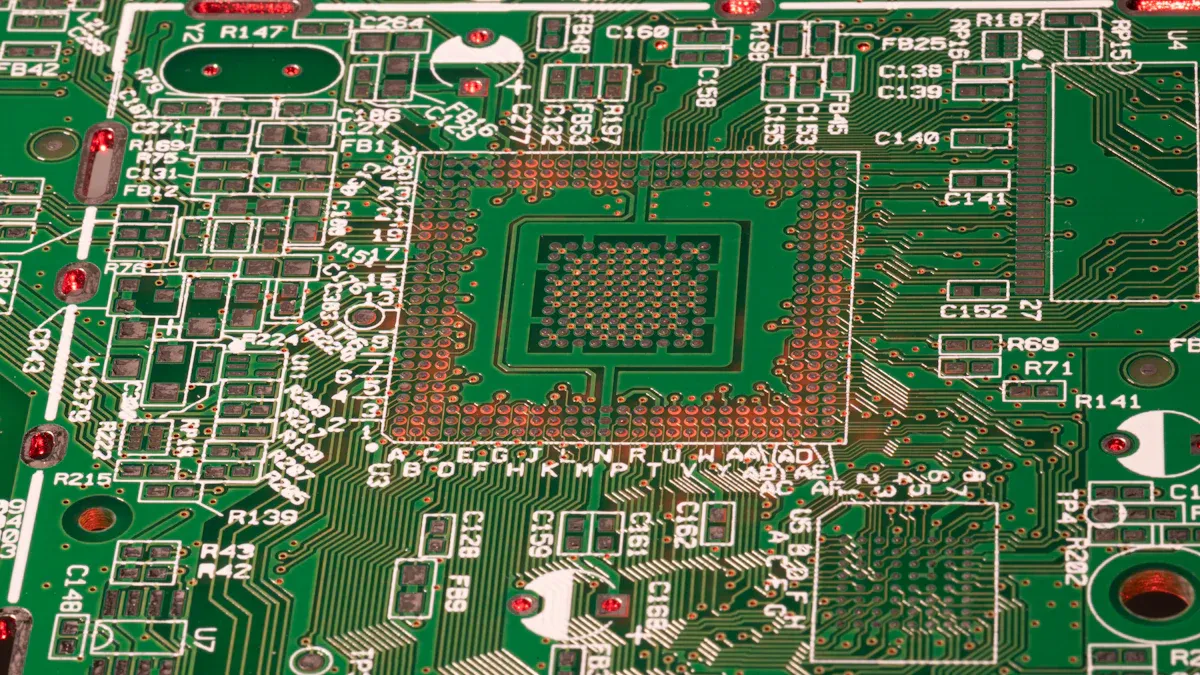
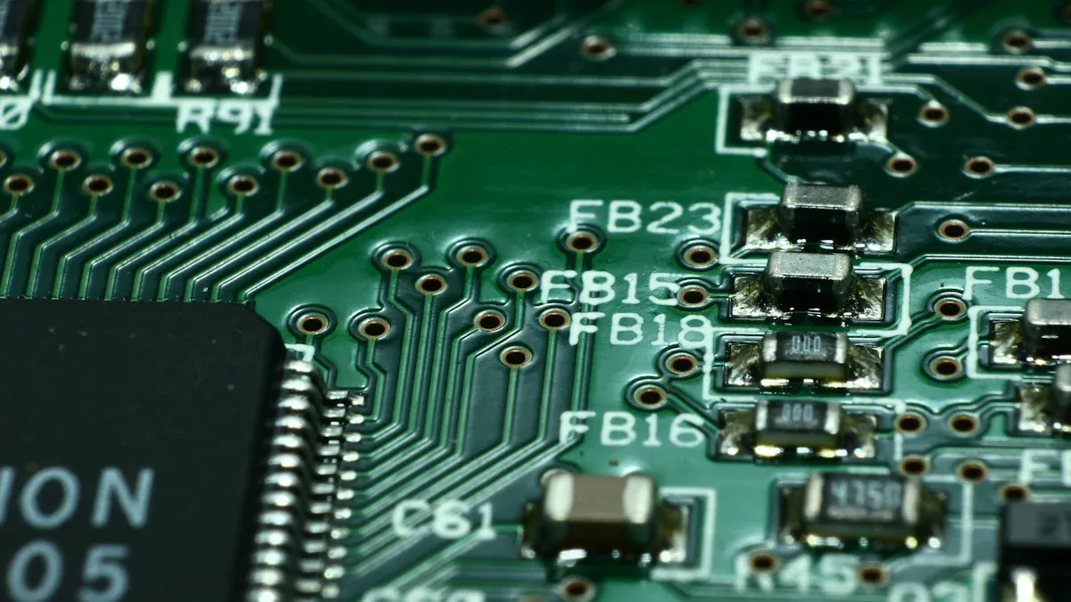
Surface Mount Technology (SMT) is a method where electronic components are mounted directly onto the surface of a printed circuit board (PCB). Unlike traditional through-hole methods, SMT eliminates the need for drilling holes into the board. This approach allows manufacturers to automate the assembly process, improving efficiency and precision.
In SMT, components such as resistors, capacitors, and integrated circuits are placed on the PCB using robotic machinery. A layer of solder paste, a mixture of solder alloy and flux, is applied to the board’s pads. The assembly then passes through a reflow oven, where heat melts the solder paste, securing the components in place. This process ensures a compact and reliable design, essential for modern electronics.
Benefits of Surface Mount Technology
Surface mount technology offers several advantages that make it indispensable in electronics manufacturing:
- Compact Design: Components are smaller and lighter, reducing the size and weight of PCBs. This compactness enhances shock and vibration resistance.
- Cost Efficiency: SMT reduces assembly costs by eliminating the need for drilled holes and speeding up production.
- Improved Reliability: Automated processes minimise human error, ensuring consistent quality.
- Faster Production: The automation of SMT significantly accelerates the manufacturing process compared to traditional methods.
These benefits have made SMT the preferred choice for industries requiring high-performance and space-efficient designs.
Applications in Electronics Manufacturing
Surface mount technology plays a critical role across various sectors:
- Consumer Electronics: Used in smartphones, tablets, and portable gaming devices.
- Automotive Electronics: Essential for engine control systems and in-car entertainment.
- Medical Devices: Found in diagnostic equipment and patient monitoring systems.
- Aerospace and Defence: Critical for applications where space and weight are constraints.
- Wearable Technology: Ideal for smartwatches and fitness trackers due to its compact nature.
| Application Area |
|---|
| Consumer Electronics |
| Telecommunication & Mobile Communication |
| Transportation and Automotive Electronics |
| Medical and Healthcare Devices |
| Aerospace & Defence Equipment |
| LED Components |
The global SMT market, valued at USD 5.27 billion, is projected to grow at a CAGR of 5.8% from 2023 to 2030. This growth reflects the increasing demand for miniaturised and efficient electronic devices.
Step-by-Step Assembly PCB SMT Process
The SMT assembly process involves several critical steps, each contributing to the creation of a reliable and efficient printed circuit board. Below is a detailed breakdown of these steps.
Solder Paste Application
The process begins with the application of solder paste onto the PCB. This paste, a mixture of solder alloy and flux, is applied to the board’s pads using a stencil. The stencil ensures that the paste is deposited only where components will be placed. Precision in this step is crucial, as any misalignment can lead to defects in the final assembly.
| Metric Type | Specification |
|---|---|
| Detection Accuracy | Z-axis resolutions as fine as 0.6 microns and height accuracy of 2 microns. |
| Comprehensive Detection | Detects short circuits, misalignment, deformation, bridging, insufficient solder, etc. |
| Solder Offset Specifications | For 01005 components, offset must be < 30% of pad length and width; for others, < 35%. |
| Solder Volume Specifications | Volume and area of solder paste must meet standards based on stencil openings. |
💡 Tip: Ensure the solder paste is stored and handled correctly to maintain its consistency and effectiveness.
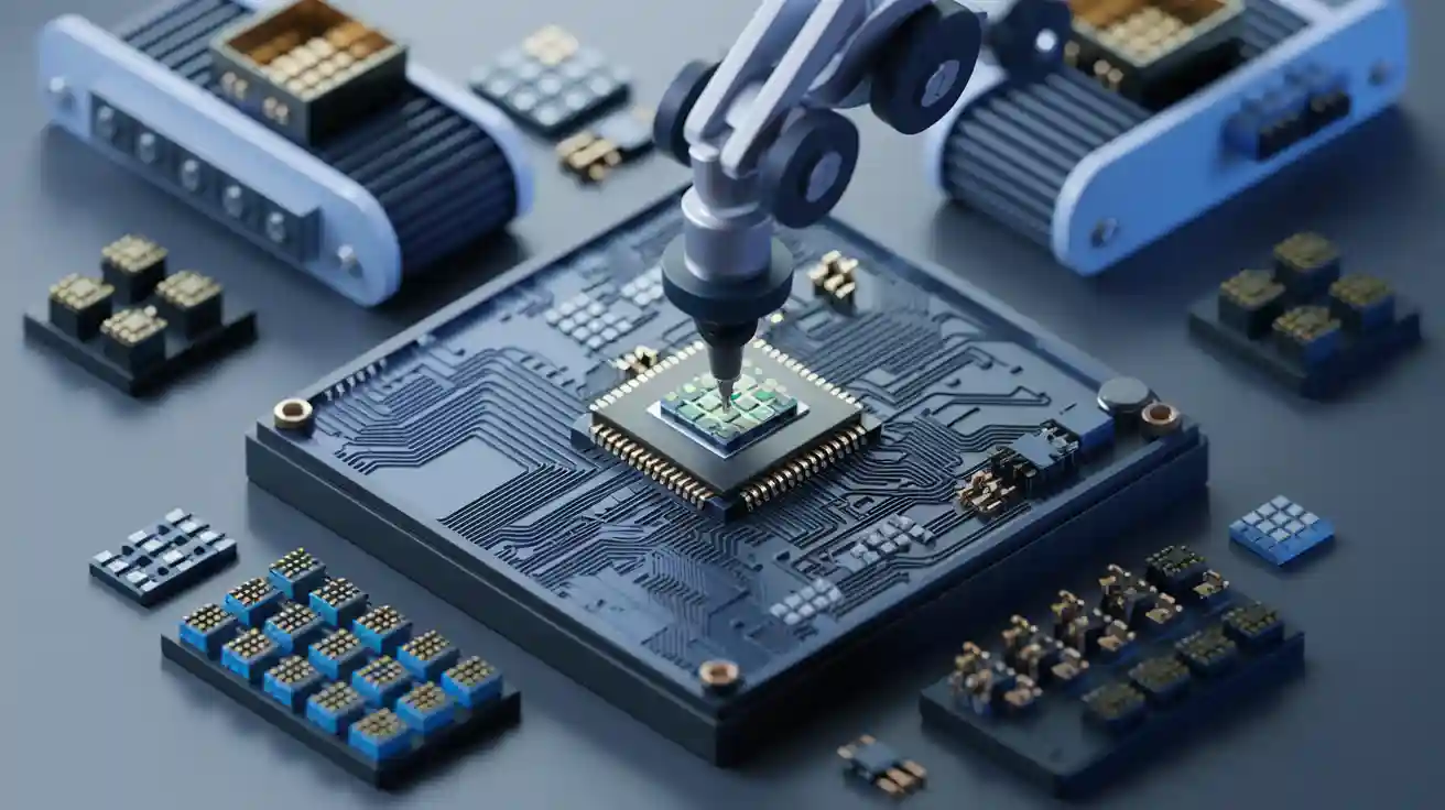
Component Placement
Once the solder paste is applied, the next step is component placement. Robotic pick-and-place machines position the components onto the PCB with high precision. These machines use vision systems to ensure components are aligned correctly with the solder paste.
- Placement accuracy statistics validate this step by ensuring components are positioned within specified tolerances.
- Accurate placement is essential for achieving reliable solder joints and maintaining overall assembly integrity.
- Inspections before and after placement verify compliance with tolerances, ensuring both components and their placements are correct.
Reflow Soldering
Reflow soldering is the process where the solder paste is melted to form permanent connections between the components and the PCB. The assembly passes through a reflow oven, which heats the board in a controlled manner.
| Temperature Stage | Typical Range | Purpose/Effect |
|---|---|---|
| Ramp Rate | 1-5°C/second | Ensures even warming to prevent thermal stresses. |
| Pre-heat Temperature | 150-160°C | Evaporates residual solvents and prevents defects from uneven heating. |
| Reflow Temperature | 30-50°C below melting point | Melts solder for proper joint formation. |
| Cooling Rate | Controlled cooling | Affects joint quality and ensures proper solidification of solder. |
Minor temperature variations can lead to defects like poor wetting and tombstoning. Tight control within a 10-30°C window is crucial for optimal thermal cycles. Consistent temperatures maximise process windows and reduce variability.
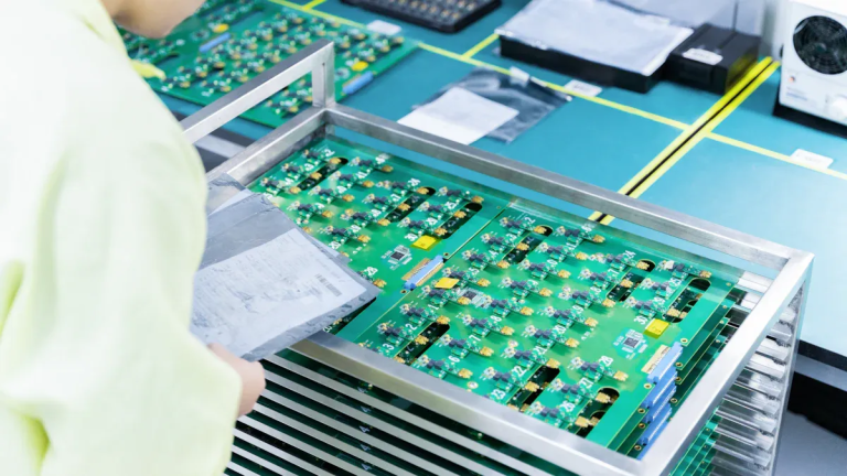
Cleaning and Inspection
After reflow soldering, the PCB undergoes cleaning to remove any flux residues or contaminants. This step ensures the board’s reliability and prevents long-term issues like corrosion. Inspection follows, where automated optical inspection (AOI) systems check for defects such as misaligned components, insufficient solder, or short circuits.
| Term | Definition |
|---|---|
| Yield | The ratio of units passing the manufacturing test to the total units entering the process. |
| Defect Level | The percentage of shipped units identified as defective by customers. |
| Test Coverage | The proportion of defects detectable during manufacturing tests compared to all possible defects. |
🔍 Note: High test coverage during inspection ensures that most defects are identified and rectified before the product reaches the customer.
Rework and Repairs
Despite the precision of the SMT assembly process, defects can still occur. Rework and repair strategies address these issues, ensuring the final product meets quality standards. Common rework tasks include removing and replacing defective components or correcting soldering errors.
- The average first-pass yield for electronics manufacturers using SMT is 80%.
- Up to 50% of soldering defects can be traced back to the solder paste printing process.
- The ’10X Rule’ highlights that rework costs increase exponentially at each stage of assembly, from $0.50 at the printing stage to $50.00 after functional testing.
🛠️ Tip: Implementing robust quality control measures during earlier stages can significantly reduce the need for costly rework.
Double-Sided Assembly PCB SMT
Differences Between Single-Sided and Double-Sided Assembly
When comparing single-sided and double-sided SMT assembly, the primary distinction lies in the number of layers used for component placement. Single-sided PCBs have components mounted on only one side, while double-sided PCBs utilise both sides of the board. This difference significantly impacts the design, complexity, and applications of the PCB.
| Characteristic | Layers | Density | Complexity | Cost | Signal Integrity | Applications |
|---|---|---|---|---|---|---|
| Single-Sided PCBs | 1 | Low | Simple | Low | Low | Simple Devices |
| Double-Sided PCBs | 2 | Medium | Moderate | Medium | Medium | Consumer Electronics |
Double-sided SMT assembly allows for higher component density and more complex circuit designs. This makes it ideal for consumer electronics, where space efficiency and functionality are critical. However, the increased complexity also requires more advanced manufacturing processes and quality control measures.
💡 Tip: If you’re designing a PCB for compact devices, double-sided SMT assembly offers the flexibility to optimise space without compromising performance.
Additional Steps for Double-Sided Assembly
Double-sided SMT assembly involves additional steps compared to single-sided assembly. These steps ensure that components on both sides are securely mounted and function as intended. The process typically includes:
- Incoming inspection to verify the quality of materials.
- Screen solder paste printing on Side A.
- Surface mounting of components on Side A.
- Drying to stabilise the solder paste.
- Reflow soldering on Side A to secure the components.
- Cleaning out any residues from Side A.
- Turning over the PCB to access Side B.
- Dispensing surface mount adhesive on Side B.
- Surface mounting of components on Side B.
- Drying to stabilise the adhesive.
- Wave soldering on Side B to secure the components.
- Cleaning out any residues from Side B.
- Visual inspection (VI) and automated optical inspection (AOI) to detect defects.
- Reworking to address any identified issues.
Each step requires precision and attention to detail. For example, the plate turnover process must be handled carefully to avoid damaging components on Side A. Similarly, wave soldering on Side B must account for the thermal impact on components already mounted on Side A.
🔍 Note: Double-sided SMT assembly demands advanced equipment and skilled operators to ensure high-quality results.
Challenges and Best Practices
Double-sided SMT assembly presents unique challenges that require careful planning and execution. Here are some common obstacles and best practices to overcome them:
- Solder Defects: Follow industry standards like IPC-2221 for clearance guidelines to minimise solder defects.
- Component Misalignment: Ensure accessible test points and avoid component obstruction to facilitate testing and repairs.
- Tombstoning: Use symmetrical pad designs and proper solder paste application to prevent tombstoning of small components.
- Panelisation: Design panels for efficient handling and ensure routing does not interfere with components.
- Minimising EMI: Implement solid ground planes and shielding to reduce electromagnetic interference.
- Silkscreen and Labelling: Ensure clear markings for component orientation to prevent assembly errors.
By adhering to these best practices, you can enhance the reliability and performance of your double-sided SMT assembly. Proper planning and quality control at each stage of the process will help you achieve optimal results.
🛠️ Pro Tip: Invest in high-quality inspection systems to identify and rectify defects early in the assembly process. This will save time and reduce costs in the long run.
Surface Mount Technology (SMT) has transformed electronics manufacturing by enabling compact, efficient, and reliable PCB designs. You benefit from faster production, reduced costs, and enhanced performance. The table below highlights the financial and operational advantages of SMT:
| Description | Potential Profit Increase |
|---|---|
| Additional hour of production time per week | $114K per year |
| Increased uptime impact on productivity | Exponential increase in gross profit |
Professionals in the field must understand SMT’s critical role. Its ability to achieve higher component density, improved electrical performance, and cost-effective assembly ensures its dominance in modern manufacturing:
| Benefit | Description |
|---|---|
| Higher component density | Enables miniaturisation and more compact designs due to tighter packing of components. |
| Enhanced electrical performance | Reduces parasitic capacitance and inductance, improving high-frequency performance. |
| Cost-effective | Faster and more automated assembly processes lead to increased production efficiency and lower labour costs. |
By mastering SMT, you can stay ahead in the rapidly evolving electronics industry.
FAQ
What is the difference between SMT and through-hole technology?
Surface Mount Technology (SMT) mounts components directly onto the PCB surface. Through-hole technology requires drilling holes for component leads. SMT offers compact designs and faster assembly.
Can SMT handle all types of electronic components?
SMT supports most components, including resistors, capacitors, and ICs. However, some large or high-power components may still require through-hole technology for better stability.
How do you ensure quality in SMT assembly?
Quality assurance involves automated optical inspection (AOI), X-ray inspection, and functional testing. These methods detect defects early and ensure the final product meets industry standards.
💡 Tip: Regular equipment calibration and skilled operators improve SMT assembly quality and efficiency.