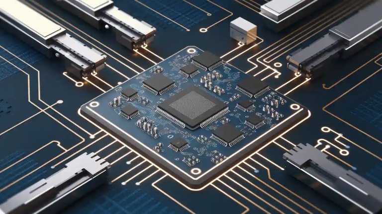
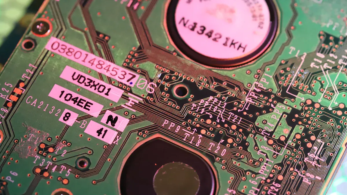
A multilayer PCB, or printed circuit board, consists of three or more layers of conductive material stacked together. This design revolutionizes modern electronics by enabling compact and efficient devices. You’ll notice its impact in products like smartphones and tablets, where space is limited, but performance is critical. The layered structure reduces the physical size of the boards while eliminating the need for bulky connectors. This not only saves space but also makes the PCB lighter, which is essential for portable and mobile devices. With multilayer PCBs, manufacturers can meet the growing demand for smaller, more powerful technology.
Key Takeaways
- Multilayer PCBs have three or more layers, making devices smaller.
- They work better by lowering signal interference and keeping signals clear.
- These PCBs are used in telecom, medical tools, and airplanes because they last long and work well.
- Even though they are useful, they cost more and are harder to make.
- Using multilayer PCBs helps your designs fit modern technology needs.
What is a Multilayer PCB?
Definition and Key Features
A multilayer PCB is a printed circuit board with three or more layers of conductive material, separated by insulating layers. These layers are stacked and bonded together, creating a compact and efficient design. Unlike single-layer or double-layer boards, multilayer PCBs allow for more complex circuitry in a smaller space. This makes them ideal for modern electronics where performance and size are critical.
Key features of multilayer PCBs include their high density, improved signal integrity, and enhanced durability. The stacked design minimizes electromagnetic interference, ensuring better performance in high-speed applications. Additionally, the internal layers are protected from environmental factors, increasing the lifespan of the board. If you’re looking for a solution that combines functionality with reliability, multilayer PCBs are the way to go.
Differences Between Multilayer and Single/Double-Layer PCBs
Understanding the differences between multilayer PCBs and their single-layer or double-layer counterparts can help you choose the right option for your needs. Here’s a quick comparison:
| Characteristic | Single-Layer PCBs | Double-Layer PCBs | Multilayer PCBs |
|---|---|---|---|
| Number of Layers | 1 | 2 | 3 or more |
| Construction | One substrate | One substrate with two conductive layers | Stacked substrates with insulation |
| Complexity | Simple | Moderate | High |
| Size | Larger | Moderate | Smaller |
| Cost | Lower | Moderate | Higher |
| Applications | Basic circuits | More complex circuits | Advanced electronics |
Multilayer PCBs stand out for their ability to support advanced electronics. They offer better quality, reliability, and performance compared to single-layer and double-layer boards. Their compact size and lightweight design make them indispensable in modern technology.
Common Applications of Multilayer PCBs
Multilayer circuit boards are used in a wide range of industries. In telecommunications, they power devices like GPS systems and satellites, where durability and functionality are essential. In the medical field, their small size and efficiency make them perfect for devices like pacemakers and imaging equipment. Automotive and aerospace industries rely on multilayer PCBs for their compactness and high-speed capabilities. Whether it’s a smartphone, laptop, or advanced defense system, multilayer PCBs are at the heart of innovation.
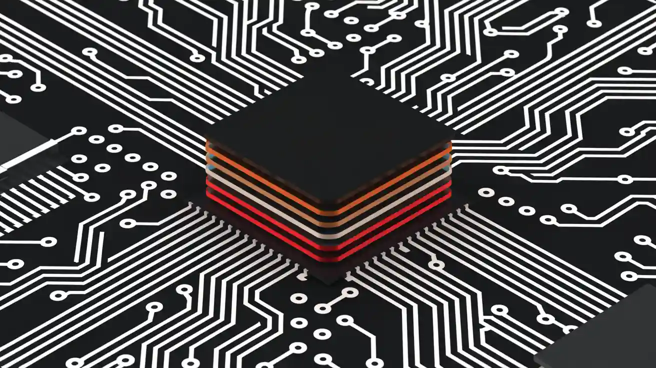
Structure of a Multilayer PCB
Layers in a Multilayer PCB
Conductive Layers
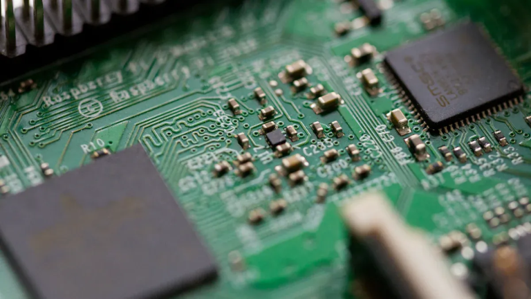
The conductive layers in a multilayer PCB are the pathways that carry electrical signals. These layers are typically made of copper, which is highly conductive and reliable. Copper foil is used to create these pathways, ensuring efficient signal transmission. The conductive layers are etched to form intricate circuit patterns, enabling the PCB to handle complex electronic functions.
Other materials, such as FR4 and Rogers PCB materials, are often used as substrates to support the copper layers. These materials provide the necessary mechanical strength and thermal stability, ensuring the board performs well under various conditions.
Insulating Layers
Insulating layers play a critical role in the structure and composition of multilayer PCBs. They separate the conductive layers, preventing electrical short circuits and maintaining signal integrity. These layers also enhance the structural integrity of the board, ensuring it remains durable and reliable.
Materials like prepreg and laminate are commonly used for insulation. Prepreg, a fiberglass cloth infused with epoxy resin, bonds the copper layers and core materials. This ensures the insulating layers can withstand heat and pressure during the lamination process, maintaining their effectiveness over time.
Key Components of a Multilayer PCB
Core
The core is the foundation of a multilayer PCB. It provides structural sturdiness and thermal resistance, ensuring the board can handle demanding applications. Typically made from fiberglass and epoxy resin, the core acts as a stable base for the other layers.
Prepreg
Prepreg is a dielectric material that binds the layers together during the lamination process. It consists of glass fibers and resin, offering excellent insulation and structural support. Prepreg also allows selective conductivity, enabling specific electrical connections while maintaining insulation elsewhere.
Copper Foil
Copper foil is essential for conducting electricity in a multilayer PCB. It forms the conductive pathways that transmit signals across the board. During manufacturing, the copper foil is etched to create the desired circuit design. This ensures the PCB can handle complex electronic tasks efficiently.
Layer Stack-Up and Design
The layer stack-up design determines the performance and reliability of a multilayer PCB. A well-structured stack-up minimizes electromagnetic interference (EMI) and enhances signal integrity. It also reduces issues like crosstalk and impedance mismatches, ensuring the board operates smoothly.
Advanced stack-up techniques include dedicated ground and power planes, which improve signal quality and reduce external noise. Proper layer arrangement also aids in thermal management, allowing the PCB to dissipate heat effectively. This is crucial for high-performance applications where reliability is key.
A carefully designed stack-up not only improves the electrical performance of the PCB but also ensures it meets the demands of modern electronics.
Multilayer PCB Manufacturing
Design and Layout
The design and layout phase is the foundation of multilayer PCB manufacturing. It ensures your PCB meets the required specifications and functions efficiently. Here’s how the process unfolds:
- Designing the CAD Model: You start by creating a detailed software model of the multilayer PCB using tools like Altium or Proteus. This step defines the circuit paths, layer stack-up, and component placement.
- Selecting a Manufacturer: Choosing the right manufacturer is crucial. You should consider factors like the maximum number of layers they can handle and their expertise in via styles.
- Manufacturing Process Planning: The manufacturer uses your design to plan the production process, including bonding prepreg and core materials under high temperature and pressure.
- Testing the PCB: After production, the PCB undergoes rigorous testing to ensure it meets performance standards.
This phase demands precision and attention to detail. A well-designed layout minimizes errors and ensures your multilayer PCB performs flawlessly.
Layer Preparation and Lamination
Layer preparation and lamination are critical steps in manufacturing multilayer PCBs. During this stage, the individual layers are carefully prepared and bonded together to form a unified structure.
- Layer Preparation: Each layer, including conductive and insulating materials, is cleaned and treated to ensure proper adhesion. Copper layers are etched to create circuit patterns, while prepreg materials are prepped for bonding.
- Lamination Process: The layers are stacked in the correct order and subjected to high temperature and pressure. This process fuses the layers into a single, durable board. The lamination ensures the layers remain aligned and maintain their structural integrity.
Proper lamination prevents delamination and ensures the board can withstand demanding applications. This step is essential for creating reliable and high-performance multilayer PCBs.
Drilling and Plating
Drilling and plating are vital for creating electrical connections between the layers of your PCB. However, this stage comes with its own set of challenges:
- Precision Requirements: Drilling must be accurate to avoid damaging the layers or misaligning the vias.
- Via Complexity: Different via types, such as through-holes, blind vias, and buried vias, offer varying levels of complexity. Through-holes are straightforward but occupy space on all layers. Blind vias increase component density, while buried vias provide the highest routing options but are the most challenging to manufacture.
- Plating Process: The drilled holes are plated with copper to establish electrical connections. This step requires stringent monitoring to ensure uniformity and avoid defects.
Drilling and plating demand advanced machinery and expertise. When done correctly, they enhance the functionality and reliability of your multilayer PCB.
💡 Tip: Partnering with an experienced manufacturer ensures precision in drilling and plating, reducing the risk of defects in your boards.
Testing and Quality Assurance
Testing and quality assurance are critical steps in ensuring your multilayer PCB performs reliably in real-world applications. Without proper testing, even the most advanced designs can fail under stress or during operation. By implementing rigorous quality checks, you can guarantee that your boards meet industry standards and deliver consistent performance.
To ensure your multilayer PCB is free from defects, manufacturers use a variety of testing methods. These include:
- Boundary Scan Testing: This method checks the interconnections between components, ensuring proper signal flow.
- Microsection Analysis: This technique investigates potential defects within the layers, such as delamination or voids.
- Solderability Testing: This test ensures that solder joints are reliable and can withstand operational stresses.
In addition to these, manufacturers often rely on advanced inspection techniques:
- Electrical testing methods, such as flying probe and bed-of-nails testing, verify the functionality of the circuits.
- X-ray inspection identifies internal defects and hidden solder joints that are not visible to the naked eye.
- Thermal stress testing evaluates the integrity of the layers under high temperatures, ensuring the board can handle demanding environments.
These tests not only identify defects but also enhance the durability and reliability of your multilayer PCB. By investing in thorough quality assurance, you can avoid costly failures and ensure your boards perform as intended.
💡 Pro Tip: Partner with a manufacturer that prioritizes quality assurance. This ensures your multilayer PCB meets the highest standards and performs flawlessly in critical applications.
Advantages and Disadvantages of Multilayer PCBs
Advantages of Multilayer PCBs
Compact Size
One of the most significant advantages of multilayer PCBs is their compact size. By stacking multiple layers, these PCBs minimize physical space while maintaining functionality. This design is essential for modern electronics, where miniaturization is key. Devices like smartphones, tablets, and wearables rely on this compactness to deliver powerful performance in a small form factor. Multilayer PCBs allow you to achieve the same capabilities as larger boards but in a much smaller and more efficient package.
High Performance
Multilayer PCBs excel in high-performance applications. Their architecture supports better signal integrity and reduces electromagnetic interference (EMI). This makes them ideal for high-speed circuits and complex electronic systems. You can also benefit from their versatility, as they meet a wide range of electrical requirements. Whether you’re designing for telecommunications, medical devices, or aerospace, these PCBs ensure optimal performance.
Enhanced Durability
Durability is another key advantage of multilayer PCBs. The internal layers are protected from environmental factors like dust, moisture, and mechanical stress. This protection extends the lifespan of the board, making it more reliable in demanding conditions. Additionally, the layered design distributes heat evenly, reducing the risk of overheating. If you need a PCB that can withstand harsh environments, multilayer PCBs are the perfect choice.
Disadvantages of Multilayer PCBs
Higher Cost
The cost of multilayer PCBs is higher compared to single-layer or double-layer boards. This is due to the sophisticated manufacturing process, which requires advanced equipment and skilled labor. Each additional layer increases material costs, and the extensive testing involved adds to the expense. While the benefits often outweigh the cost, you should consider your budget when choosing a multilayer PCB.
Complex Manufacturing Process
Manufacturing multilayer PCBs is a complex and time-consuming process. Precise alignment and lamination of the layers are critical to ensure functionality. The intricate design requires specialized machinery and expertise, which can lead to longer production times. If you’re working on a tight schedule, this complexity might pose a challenge.
Repair Challenges
Repairing multilayer PCBs can be difficult. Accessing the inner layers without damaging the board is a significant challenge. The complexity of the design makes troubleshooting and repairs more time-intensive and costly. If a multilayer PCB fails, replacing it is often more practical than attempting repairs. This is something you should keep in mind when considering these boards for your project.
💡 Tip: To minimize repair issues, partner with a reliable manufacturer who prioritizes quality assurance during production.
Applications of Multilayer PCBs
Consumer Electronics
Multilayer PCBs have transformed the consumer electronics industry. You’ll find them in devices like smartphones, tablets, and laptops, where compactness and efficiency are essential. These boards allow manufacturers to pack numerous circuits into a small space, enabling sleek designs without compromising functionality.
Modern appliances like smart TVs, microwaves, and washing machines also rely on multilayer PCBs. Their ability to handle complex circuitry ensures these devices perform multiple tasks seamlessly. Home automation systems, including smart thermostats and security cameras, benefit from the reliability and durability of these boards.
💡 Did you know? Multilayer PCBs are the backbone of portable gadgets like shaving machines and irons, making them more efficient and user-friendly.
Telecommunications
In telecommunications, multilayer PCBs play a critical role in maintaining high performance. They are essential for devices like satellites, mobile phone repeaters, and GPS systems. These boards ensure reliable signal transmission, even in demanding environments.
Telecommunication towers and radar electronics also depend on multilayer PCBs for their durability and functionality. Their compact design supports the development of sophisticated, miniature devices used in wireless technologies. Whether it’s a power amplifier or an attenuator, these PCBs meet the high-performance demands of modern communication systems.
📡 Pro Tip: If you’re designing for telecommunications, multilayer PCBs provide the durability and precision needed for outdoor and mobile applications.
Medical Devices
The medical field relies heavily on multilayer PCBs to create compact and lightweight devices. These boards enable advanced medical equipment like MRI machines, CT scanners, and X-ray systems to function efficiently. Their ability to support intricate circuitry is vital for non-invasive treatments and diagnostic tools.
You’ll also find multilayer PCBs in portable devices like blood pressure monitors and sugar testing kits. Their reliability ensures accurate readings, which are crucial for patient care. From heart monitors to infrared temperature sensors, these PCBs enhance the functionality of life-saving equipment.
🏥 Note: Multilayer PCBs are indispensable in modern healthcare, ensuring precision and reliability in critical applications.
Automotive Industry
The automotive industry has embraced multilayer PCBs to meet the growing demand for smarter, more efficient vehicles. These boards are essential for modern automotive electronics, offering compactness, durability, and high functionality. Their ability to withstand extreme temperatures and vibrations makes them ideal for the demanding internal environment of vehicles.
You’ll find multilayer PCBs in critical systems like engine control units (ECUs), anti-lock braking systems (ABS), and advanced driver-assistance systems (ADAS). These systems rely on the compact design of multilayer boards to integrate multiple circuits into a small space, ensuring seamless performance. Additionally, their heat resistance enhances reliability, even under intense operating conditions.
🚗 Did you know? Multilayer PCBs are also used in electric vehicles (EVs) to manage battery systems and power distribution. Their efficiency contributes to the overall performance and safety of EVs.
By choosing multilayer PCBs for your automotive designs, you can achieve higher functionality without compromising on space or durability. These boards are the backbone of innovation in the automotive sector, enabling the development of smarter, safer, and more efficient vehicles.
Aerospace and Defense
In aerospace and defense, multilayer PCBs play a pivotal role in advancing technology. Their compact design and exceptional functionality make them indispensable for high-speed circuits and critical applications. These boards allow for more room to add components, enhancing the performance of complex systems.
Multilayer PCBs are used in a wide range of aerospace and defense technologies, including:
- Unmanned Aerial Vehicles (UAVs) and Ground Vehicles (UGVs)
- Aircraft defense systems and avionics
- Surveillance systems and radar systems
- Automated weapons and nuclear systems
Their durability ensures reliable performance in extreme conditions, such as high altitudes and harsh environments. For example, in radar systems, multilayer PCBs provide the precision and speed required for accurate signal processing. Similarly, in UAVs, their lightweight and compact design improve flight efficiency and functionality.
✈️ Pro Tip: If you’re designing for aerospace or defense, multilayer PCBs offer the reliability and performance needed for mission-critical applications.
By integrating multilayer PCBs into your aerospace and defense projects, you can achieve unparalleled performance and reliability. These boards are the cornerstone of innovation in industries where precision and durability are non-negotiable.
Multilayer PCBs have revolutionized the electronics industry with their compact, lightweight, and high-performance design. By stacking multiple conductive and insulating layers, these boards deliver unmatched functionality in a smaller footprint. Their durability and reliability make them indispensable for industries like telecommunications, medical devices, and aerospace. You benefit from their ability to simplify designs, reduce weight, and enhance electrical performance.
As technology evolves, multilayer PCBs continue to drive innovation. From enabling 5G connectivity to powering IoT devices, they are at the forefront of modern advancements. By choosing multilayer PCBs, you ensure your designs meet the demands of today’s fast-paced, technology-driven world.
🌟 Takeaway: Multilayer PCBs are not just a choice but a necessity for creating powerful, efficient, and future-ready electronic devices.
FAQ
What makes multilayer PCBs better than single-layer boards?
Multilayer PCBs offer higher performance, compact size, and better signal integrity. They handle complex circuits in smaller spaces, making them ideal for advanced electronics. If you want a reliable, high-performing solution for modern devices, multilayer PCBs are the way to go.
Are multilayer PCBs suitable for high-temperature environments?
Yes, multilayer PCBs are designed to withstand extreme temperatures. Their materials, like FR4 and prepreg, provide excellent thermal resistance. This makes them perfect for industries like automotive and aerospace, where durability under heat is critical.
How do multilayer PCBs reduce electromagnetic interference (EMI)?
Multilayer PCBs use dedicated ground and power planes to minimize EMI. These planes shield signals from external noise, ensuring better performance. If your project requires high-speed circuits, this feature is essential for maintaining signal integrity.
Can multilayer PCBs be customized for specific applications?
Absolutely! You can customize the layer stack-up, materials, and via types to meet your project’s needs. Whether it’s for medical devices or telecommunications, multilayer PCBs offer flexibility to match your requirements.
Are multilayer PCBs worth the higher cost?
Yes, they are worth it. Their compact size, durability, and high performance justify the investment. If you prioritize reliability and efficiency in your designs, multilayer PCBs deliver unmatched value for advanced applications.
💡 Tip: Partner with a trusted manufacturer to ensure your multilayer PCB meets your exact specifications and quality standards.